
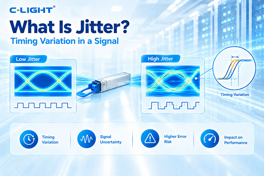
Jitter is the unwanted variation in the timing of a digital signal relative to its ideal timing position. It is an important signal-integrity parameter in high-speed electrical and optical communication because excessive jitter reduces timing margin, distorts the eye diagram, and can increase bit or symbol errors.
Jitter is the short-term variation in the timing of signal transitions from their ideal locations.
In an ideal digital signal, transitions occur at precise and equally spaced time intervals. In a real system, noise, interference, clock instability, reflections, and other impairments can cause transitions to move earlier or later than expected.
A simplified signal path is:
Data Source → Driver → Electrical or Optical Channel → Receiver → Sampling Decision
Jitter changes the timing of signal transitions along this path. When the receiver samples the signal, excessive timing variation can cause the sampling point to move too close to a transition, increasing the probability of an incorrect decision.
Jitter directly affects timing margin. When jitter becomes large, the valid sampling window becomes smaller.
This is especially important for high-speed interfaces such as 400G, 800G, and 1.6T systems, where unit intervals become shorter and timing margins become tighter.
An ideal digital signal has transitions that occur at precisely defined time positions. Each symbol or bit interval has a fixed duration and the receiver can sample the signal at a predictable point.
Real systems always contain some amount of timing variation, so jitter is normally a matter of controlling it within acceptable limits rather than eliminating it completely.
Jitter is commonly divided into two major categories:
Random Jitter (RJ)
Deterministic Jitter (DJ)
Total jitter can also be described using a combination of random and deterministic components depending on the measurement methodology.
Random jitter is a stochastic timing variation that is generally associated with random physical noise sources.
Typical causes can include thermal noise, shot noise, and other statistically random processes. Random jitter is commonly modeled using a probability distribution and does not have a fixed repeating pattern.
Deterministic jitter is timing variation associated with identifiable and bounded causes. Unlike random jitter, it can often be traced to a specific source or repeating mechanism.
Examples include data-dependent effects, periodic interference, crosstalk, and duty-cycle distortion.
Total jitter represents the combined timing uncertainty considered in a particular measurement or system model.
It can include both random and deterministic components. The exact method used to calculate or extrapolate total jitter depends on the applicable test methodology.
Data-dependent jitter, or DDJ, is timing variation that depends on the transmitted data pattern.
It is commonly associated with inter-symbol interference and frequency-dependent channel loss. Different preceding symbols can cause signal transitions to occur at slightly different times.
Periodic jitter is a timing variation that repeats at a specific frequency or a set of related frequencies.
It can be caused by clock coupling, switching power supplies, reference-clock interference, or other periodic noise sources.
Duty-cycle distortion occurs when the durations of logical high and low states are not equal as expected.
This can shift signal transition timing and contribute to deterministic jitter in high-speed interfaces.
Bounded uncorrelated jitter refers to a type of deterministic timing variation that has a limited amplitude but is not necessarily correlated with the transmitted data.
It can be caused by periodic interference or other bounded timing disturbances.
Jitter is commonly expressed as a unit of time, such as:
Seconds
Picoseconds (ps)
Femtoseconds (fs)
Jitter can also be normalized to the symbol period or expressed as a unit interval (UI).
A Unit Interval is the nominal duration of one symbol period in a serial communication system.
Expressing jitter in UI allows timing variation to be compared relative to the signal speed. As data rates increase, one UI becomes shorter, so the same absolute timing error represents a larger fraction of the available timing margin.
A simple timing-error representation is:
Jitter = Actual Transition Time − Ideal Transition Time
For example, if an ideal transition occurs at 100ps and the actual transition occurs at 103ps, the instantaneous timing error is 3ps.
Actual jitter specifications normally require a defined statistical or measurement methodology rather than a single transition measurement.
Higher data rates mean shorter symbol periods. Therefore, even a small absolute timing error can consume a larger fraction of the available timing margin.
This makes jitter control increasingly important as systems move from 100G to 400G, 800G, and 1.6T.
Jitter primarily appears as horizontal spreading of signal transitions in an eye diagram.
As jitter increases, the horizontal eye opening becomes smaller, reducing the available timing margin for the receiver.
Horizontal eye closure refers to the reduction in the usable timing window caused by jitter and other time-domain impairments.
A smaller horizontal eye opening indicates that the receiver has less freedom to choose an optimal sampling time.
Excessive jitter can move signal transitions closer to the receiver sampling point, increasing the probability of incorrect bit or symbol decisions.
As a result, higher jitter can contribute to a higher BER, particularly when the system is already operating near its timing margin.
PAM4 uses four amplitude levels and therefore has tighter signal margins than two-level NRZ signaling.
Jitter affects the horizontal timing margin of each PAM4 eye. As the eye openings become narrower, the receiver has less timing margin for reliable symbol detection.
PAM4 is used to increase the number of bits transmitted per symbol, but it operates with tighter overall signal margins.
High-speed PAM4 systems must therefore control timing variation together with amplitude noise, inter-symbol interference, crosstalk, and other signal impairments.
| Feature | Jitter | Noise |
|---|---|---|
| Primary effect | Timing variation | Amplitude or signal-level variation |
| Eye diagram | Mainly horizontal spreading | Mainly vertical spreading |
| Typical unit | ps, fs, UI | V, mV, dB, or other noise metrics |
Jitter describes variation in the timing of transitions, while inter-symbol interference occurs when one symbol affects another because of channel memory and bandwidth limitations.
ISI can produce data-dependent timing shifts and therefore can contribute to deterministic jitter.
High-frequency channel loss changes the shape and timing of fast signal transitions. As the waveform is filtered by the channel, different data patterns can produce different transition positions.
This pattern-dependent timing variation is one important source of data-dependent jitter.
Impedance mismatches can reflect electrical energy back toward the transmitter. The reflected waveform can combine with the main signal and alter the timing of subsequent transitions.
This can create deterministic timing variation and reduce the eye opening.
Crosstalk from neighboring high-speed channels can disturb the timing of signal transitions. Depending on the source and coupling mechanism, this disturbance can appear as deterministic or pattern-related jitter.
Reducing crosstalk is therefore important for maintaining timing margin in dense high-speed systems.
The reference clock provides timing information for many high-speed systems. Instability or phase noise in the clock can be transferred into the data path.
A low-jitter clock source helps maintain stable timing throughout the communication system.
Phase noise describes short-term fluctuations in the phase of an oscillator or clock signal. In a data communication system, phase noise can contribute to timing uncertainty and therefore affect jitter performance.
Optical transceivers contain electrical drivers, optical transmitters, receivers, TIAs, DSPs, and host-facing interfaces. Timing variation can be introduced or accumulated across these components.
Maintaining low jitter is particularly important for high-speed electrical and optical interfaces using PAM4 signaling.
Transmitter timing jitter can cause optical signal transitions to occur at different times than expected.
Excessive transmitter jitter can reduce the timing margin available to the receiving system and contribute to degraded BER performance.
The receiver must sample the incoming signal at an appropriate time. Jitter reduces the certainty of the transition locations and therefore reduces the available sampling window.
A receiver with limited timing margin may become more sensitive to additional jitter introduced by the channel or transmitter.
Receiver sensitivity primarily describes the minimum optical power required to achieve a specified performance. Jitter describes timing variation.
They measure different aspects of link performance, but both can affect BER and the overall operating margin.
RIN, or Relative Intensity Noise, represents fluctuations in optical power, while jitter represents timing fluctuations.
RIN mainly affects amplitude noise, whereas jitter primarily affects timing margin. Both can contribute to signal degradation in high-speed optical systems.
Extinction ratio describes the optical power relationship between high and low states in a two-level optical signal. Jitter describes transition timing variation.
They are separate transmitter parameters, but both can affect the quality of the signal seen by the receiver.
TDECQ is an optical transmitter performance metric used for applicable PAM4 systems, while jitter describes timing variation.
Jitter can contribute to eye closure and therefore influence overall PAM4 transmitter performance, but TDECQ is not simply a jitter measurement.
Jitter is commonly measured using a high-bandwidth oscilloscope or dedicated bit-error-rate and jitter-analysis equipment.
A typical measurement involves capturing a large number of signal transitions and statistically analyzing their timing relative to the ideal reference.
Common test equipment includes:
High-bandwidth oscilloscope
Sampling oscilloscope
Bit Error Rate Tester
Pattern generator
Clock source
Jitter-analysis software
Random jitter is commonly characterized using statistical analysis of transition timing. The measured distribution can be used to estimate parameters associated with the random component.
Because random jitter is unbounded in an ideal statistical model, the reported value depends on the defined measurement and extrapolation method.
Deterministic jitter can be analyzed by identifying bounded timing variations and separating them from random components.
Data-dependent jitter, periodic jitter, and duty-cycle distortion may be analyzed individually depending on the test methodology.
Total jitter measurement combines relevant timing-error components according to a defined methodology.
For high-speed interfaces, the measurement may include random jitter, deterministic jitter, data-dependent jitter, periodic jitter, and other specified components.
400G systems commonly use high-speed PAM4 lanes. Jitter testing evaluates the timing stability of the electrical or optical waveform and verifies that the interface maintains sufficient timing margin.
Testing can be performed at the transmitter, receiver, or complete link depending on the validation objective.
800G optical systems use multiple high-speed lanes, commonly based on 100G-class PAM4 signaling. The timing margin on each lane must be carefully controlled.
Jitter measurements help identify clock quality, channel loss, reflections, crosstalk, and other timing-related impairments.
As lane speeds increase toward 200G-class signaling, each symbol period becomes shorter and timing margins become more demanding.
Small amounts of absolute timing variation can therefore consume a significant portion of the available UI, making jitter control increasingly important.
Jitter can be reduced by improving the clock, electrical channel, transmitter, receiver, and overall system design.
Use a low-jitter reference clock
Optimize PCB and cable routing
Reduce impedance discontinuities
Control crosstalk
Improve equalization
Reduce power-supply noise
Optimize transmitter and receiver components
DSP can compensate for certain deterministic signal impairments and recover timing information from the received waveform.
However, DSP cannot eliminate all physical sources of timing noise. Good clock, channel, and component design remain essential.
FEC can correct certain bit errors after the physical signal has been received, but it does not directly remove the timing variation that caused those errors.
Jitter should therefore be controlled at the physical layer, while FEC provides additional error-correction capability at the communication-system level.
Excessive jitter can cause:
Reduced horizontal eye opening
Lower timing margin
Higher BER
Increased symbol errors
Reduced link reliability
Lower operating margin
As optical and electrical interfaces move toward 800G and 1.6T, timing margins will become increasingly challenging. Jitter control will require improvements in clocks, SerDes, optical transmitters, receivers, DSP, packaging, PCB design, and test technology.
Jitter is the unwanted variation in signal timing that reduces the available sampling window in high-speed communication systems. It can originate from clocks, electrical channels, transmitters, receivers, reflections, crosstalk, and other sources. Random and deterministic jitter are the two main categories. In PAM4-based 400G, 800G, and 1.6T systems, controlling jitter is essential for maintaining eye opening, timing margin, low BER, and reliable high-speed optical communication.
For any questions, please contact us by email or WhatsApp.
Email: sales@c-light.com
WhatsApp: +86 132 6656 7067